- 您现在的位置:买卖IC网 > Sheet目录1997 > ICS8430S07AKILF (IDT, Integrated Device Technology Inc)IC CLK GENERATOR PLL 32VFQFN
ICS8430S07AKI REVISION A SEPTEMBER 3, 2009
15
2009 Integrated Device Technology, Inc.
ICS8430S07I Data Sheet
CLOCK GENERATOR FOR CAVIUM PROCESSORS
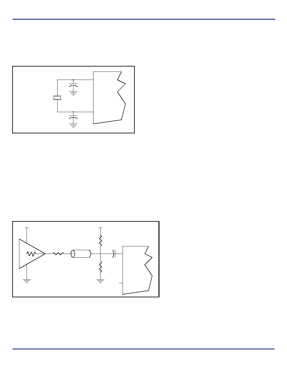
Crystal Input Interface
The ICS8430S07I has been characterized with 18pF parallel
resonant crystals. The capacitors C1 and C2 are not required, but
can be populated for optimal ppm accuracy. The C1 and C2 values
can be slightly adjusted to minimize ppm error for different board
layouts.
Figure 4. Crystal Input Interface
LVCMOS to XTAL Interface
The XTAL_IN input can accept a single-ended LVCMOS signal
through an AC coupling capacitor. A general interface diagram is
shown in Figure 5. The XTAL_OUT pin can be left floating. The input
edge rate can be as slow as 10ns. For LVCMOS signals, it is
recommended that the amplitude be reduced from full swing to half
swing in order to prevent signal interference with the power rail and
to reduce noise. This configuration requires that the output
impedance of the driver (Ro) plus the series resistance (Rs) equals
the transmission line impedance. In addition, matched termination at
the crystal input will attenuate the signal in half. This can be done in
one of two ways. First, R1 and R2 in parallel should equal the
transmission line impedance. For most 50
applications, R1 and R2
can be 100
. This can also be accomplished by removing R1 and
making R2 50
. By overdriving the crystal oscillator, the device will
be functional, but note, the device performance is guaranteed by
using a quartz crystal.
Figure 5. General Diagram for LVCMOS Driver to XTAL Input Interface
XTAL_IN
XTAL_OUT
X1
18pF Parallel Crystal
C1
Spare
C2
Spare
XTAL_IN
XTAL_OUT
Ro
Rs
Zo = Ro + Rs
50
0.1f
R1
R2
VDD
发布紧急采购,3分钟左右您将得到回复。
相关PDF资料
ICS8430S10BYI-02LF
IC CLK GENERATOR PLL 48TQFP
ICS84314AY-02LFT
IC SYNTHESIZER 700MHZ 32-LQFP
ICS843156AKILF
IC CLK GENERATOR 32VFQFP
ICS843156AKLF
IC CLK GENERATOR 32VFQFP
ICS843202AYILF
IC SYNTHESIZER 680MHZ 32-LQFP
ICS843204AGILF
IC SYNTHESIZER LVPECL 48-TSSOP
ICS84320AY-01LN
IC SYNTHESIZER GP LVPECL 32-LQFP
ICS84320AYI-01LF
IC FREQ SYNTHESIZER 32TQFP
相关代理商/技术参数
ICS8430S07AKILFT
功能描述:IC CLK GENERATOR PLL 32VFQFN RoHS:是 类别:集成电路 (IC) >> 时钟/计时 - 专用 系列:- 标准包装:1,500 系列:- 类型:时钟缓冲器/驱动器 PLL:是 主要目的:- 输入:- 输出:- 电路数:- 比率 - 输入:输出:- 差分 - 输入:输出:- 频率 - 最大:- 电源电压:3.3V 工作温度:0°C ~ 70°C 安装类型:表面贴装 封装/外壳:28-SSOP(0.209",5.30mm 宽) 供应商设备封装:28-SSOP 包装:带卷 (TR) 其它名称:93786AFT
ICS8430S07I
制造商:IDT 制造商全称:Integrated Device Technology 功能描述:Clock Generator for Cavium Processors
ICS8430S10AYILF
功能描述:IC CLK GENERATOR PLL 48TQFP RoHS:是 类别:集成电路 (IC) >> 时钟/计时 - 专用 系列:- 标准包装:1,500 系列:- 类型:时钟缓冲器/驱动器 PLL:是 主要目的:- 输入:- 输出:- 电路数:- 比率 - 输入:输出:- 差分 - 输入:输出:- 频率 - 最大:- 电源电压:3.3V 工作温度:0°C ~ 70°C 安装类型:表面贴装 封装/外壳:28-SSOP(0.209",5.30mm 宽) 供应商设备封装:28-SSOP 包装:带卷 (TR) 其它名称:93786AFT
ICS8430S10AYILFT
功能描述:IC CLK GENERATOR PLL 48TQFP RoHS:是 类别:集成电路 (IC) >> 时钟/计时 - 专用 系列:- 标准包装:1,500 系列:- 类型:时钟缓冲器/驱动器 PLL:是 主要目的:- 输入:- 输出:- 电路数:- 比率 - 输入:输出:- 差分 - 输入:输出:- 频率 - 最大:- 电源电压:3.3V 工作温度:0°C ~ 70°C 安装类型:表面贴装 封装/外壳:28-SSOP(0.209",5.30mm 宽) 供应商设备封装:28-SSOP 包装:带卷 (TR) 其它名称:93786AFT
ICS8430S10BYI-02LF
功能描述:IC CLK GENERATOR PLL 48TQFP RoHS:是 类别:集成电路 (IC) >> 时钟/计时 - 专用 系列:- 标准包装:1,500 系列:- 类型:时钟缓冲器/驱动器 PLL:是 主要目的:- 输入:- 输出:- 电路数:- 比率 - 输入:输出:- 差分 - 输入:输出:- 频率 - 最大:- 电源电压:3.3V 工作温度:0°C ~ 70°C 安装类型:表面贴装 封装/外壳:28-SSOP(0.209",5.30mm 宽) 供应商设备封装:28-SSOP 包装:带卷 (TR) 其它名称:93786AFT
ICS8430S10BYI-02LFT
功能描述:IC CLK GENERATOR PLL 48TQFP RoHS:是 类别:集成电路 (IC) >> 时钟/计时 - 专用 系列:- 标准包装:1,500 系列:- 类型:时钟缓冲器/驱动器 PLL:是 主要目的:- 输入:- 输出:- 电路数:- 比率 - 输入:输出:- 差分 - 输入:输出:- 频率 - 最大:- 电源电压:3.3V 工作温度:0°C ~ 70°C 安装类型:表面贴装 封装/外壳:28-SSOP(0.209",5.30mm 宽) 供应商设备封装:28-SSOP 包装:带卷 (TR) 其它名称:93786AFT
ICS8430S10I-03
制造商:IDT 制造商全称:Integrated Device Technology 功能描述:Clock Generator for Cavium Processors
ICS8431-01
制造商:ICS 制造商全称:ICS 功能描述:200MHZ, LOW JITTER, LVPECL FREQUENCY SYNTHESIZER